Copyright © 1997 Derek Mc Donnell.
All Rights Reserved.
Last updated 15-Mar-1998.

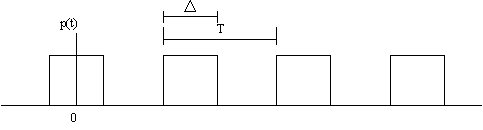
Pulse Amplitude Modulation uses a carrier signal which is a pulse train,
as illustrated in Figure 1.0.
Amplitude modulation of this type is referred to as pulse amplitude
modulation (PAM).
One of the important applications of pulse amplitude modulation is for
transmission of several signals over a single channel.
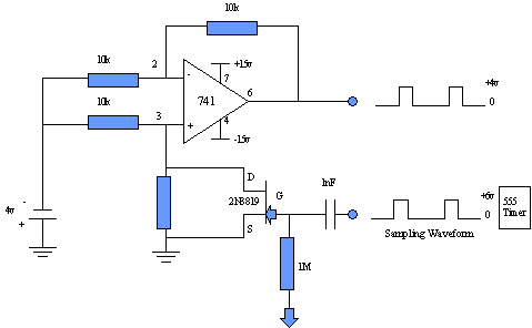
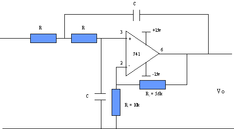
Pulse amplitude modulation systems are analog systems and share a common
problem with AM and FM modulation systems. That is, each of these analog
modulation systems are extremely sensitive to the noise present in the
receiver.
By converting the analog signal into a digital signal prior to modulation
(such a conversion is called source encoding) we will see that when the
digital signal is modulated and transmitted, the received signal will be far
less sensitive to the receiver noise than an analog modulation.

Procedure

1)	Build the 555 Timer circuit as shown in Figure 1.0.

2)	For the given values of the following components calculate f:

	C1 = 0.0F			R1 = 4k3
	R1 + R2 = 10k			R2 = 2k7
	f  10kHz			C1 + C2 = 0.01F

3)	Now build the PAM Modulator circuit using the 555 Timer for the
	sampling waveform.

4)	Replace the 4v DC with 4v AC.
	Examine the output for different frequencies f < fs,	f = fs 	and 	f > fs.
5)	Connect the output of Figure 2.0 into Figure 3.0.
	Where R = 2.2k,	C = 0.1F
	This circuit is a second order lowpass Butterworth filter.
	fc = 1/2RC = 720Hz with a Voltage gain of 1.56.
	You may need to adjust the R2 resistor in the 555 Timer.
Hard - Wired Telemetry System
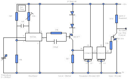
Introduction This report describes a Hard - Wired Telemetry System. The aim is to monitor the capacitance of a slow - moving, remote electrical transducer: such devices are quite often found in position sensors, pressure measuring equipment and liquid depth sensors. The process of monitoring physical parameters at a distance is known as telemetry. Telemetry Telemetry may be defined as remote metering. It is the process of gathering data on some particular phenomenon without the presence of human monitors. The gathered data may be recorded on chart recorders, tape recorders or computer memory and then picked up at some convenient time. If the data is transmitted as a radio wave it is called radio telemetry. Overview In the experiment the transmission medium used was a wire line or cable. Other types of communication links could have been used e.g. infra-red, ultrasonic, or radio transmitters/receivers. To simulate the sensor a standard laboratory capacitor substitution box was used. The input values were manually selected. A the transmitter there is a circuit to convert the variable capacitance to a related audio-frequency square wave. This is used to drive the transmission line to the distant receiver. The frequency-modulated input to the receiver is converted back to a voltage representing the instantaneous value of the capacitance, ready for display on an appropriately scaled meter or paper strip recorder. Objectives The basic objectives to be fulfilled in this experiment are therefore as follows: 1) To discuss, and where appropriate analyse, the operation of each stage in the telemeter, given the underlying circuit designs. 2) To produce a final calibration law for the system in the form of a graph relating the filter output voltage to the sensor capacitance.

Transmitter

Procedure:

1)	Build the transmitter stage first - circuit details are shown in
	Figure 2.0.
	Construct and test the transmitter on a stage by stage basis,
	starting with the oscillator.
	Identify the function of each component and note the signal levels and
	waveforms where appropriate.

2)	A Signetics NE566 is used as a capacitance controlled oscillator.
	Many larger capacitive transducers have operational ranges of
	between about 200 - 2000pF.
	With such values oscillators running directly at audio frequency
	(to be compatible with the telephone line as a communication link, for
	example) would not have sufficient sensitivity.
	Allowing the oscillator to operate in the higher 30 - 300kHz band
	returns an adequate sensitivity: a divide-by-100 circuit outputs the
	desired audio frequency signal. A bipolar drive stage interfaces the
	divider output to the line.

3)	Produce a calibration graph for the transmitter, relating the
	frequency of the output wave to the input capacitance.
	Is the shape of the graph satisfactory ?
	How does the shape correspond with information given on the
	NE566 data sheet ?

4)	Note and explain what happens when a length of transmission line is
	connected to the transmitter's output.
The 555 timer is a very versatile and widely used device because it can be configured in two different modes as either a monostable multivibrator (one-shot) or as an astable multivibrator (oscillator). An astable multivibrator has no stable states and therefore changes back and forth (oscillates) between two unstable states without any external triggering.
A functional diagram showing the internal components of a 555 timer is given in Figure 1.0 below. Basic Internal Operation of the 555 Timer
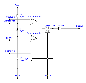
Operational amplifiers are constructed to act as comparators whose outputs are
HIGH when the voltage on the positive (+) input is greater than the voltage on
the negative (-) input and LOW when the - input is greater than the + input.
The voltage divider consisting of three 5k resistors provides a trigger level
of 1/3Vcc and a threshold level of 2/3Vcc. The control voltage input can be
used to externally adjust the trigger and threshold values to other values if
necessary.
When the normally HIGH trigger input momentarily goes below 1/3Vcc, the
output of comparator B switches from LOW to HIGH and sets the S-R latch,
causing the output (pin 3) to go HIGH and turning the discharge transistor Q1
off.
The output will stay HIGH until the normally LOW threshold input goes above
2/3Vcc and causes the output of comparator A to switch from LOW to HIGH.
This resets the latch causing the output to go back LOW and turning the
discharge transistor on. The external reset input can be used to reset the
latch independent of the threshold circuit. The trigger and the threshold
inputs are controlled by external components connected to produce either
monostable or astable action.
A 555 timer connected to operate as an astable multivibrator, which is a
free-running non sinusoidal oscillator, is shown in Figure 1.1. The threshold
input is now connected to the trigger input. Initially, when the power is
turned on, the capacitor C1 is uncharged and thus the trigger voltage is at 0v.
This causes the output of compatator B to be HIGH and the output of
comparator A to be LOW, forcing the output of the latch, and thus the base
of Q1, LOW and keeping the transistor off. Now, C1 begins charging
through R1 and R2. When the capacitor voltage reaches 1/3Vcc,
comparator B switches to its LOW output state, and when the capacitor
voltage reaches 2/3Vcc, comparator A switches to its HIGH output state.
This resets the latch, causing the base of Q1 to go HIGH, and turns on the
transistor. This sequence creates a discharge path for the capacitor through
R2 and the transistor. The capacitor now begins to discharge, causing
comparator A to go LOW. At the point where the capacitor discharges
down to 1/3Vcc, comparator B switches HIGH, setting the latch, which
makes the base of Q1 LOW and turns off the transistor. Another charging
cycle begins, and the entire process repeats.
The result is a rectangular wave output whose duty cycle depends on the
values of R1 and R2.
The frequency of oscillation is given by the following formula:
f = 1.44/(R1+2R2)C1
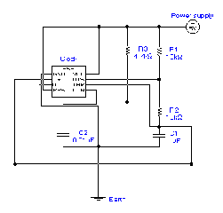
The below diagram shows the 555 timer as captured from Electronic Work Bench.

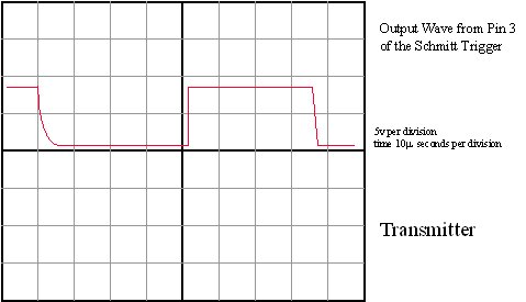
The output wave of pin 3 of the Schmitt trigger is basically a square wave.
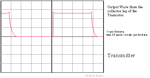
The output wave from the collector leg of the Transistor is almost square but
the edges have spikes and have been degraded in quality.
The output wave from the first divide by 10 chip is similar to the input
waveform with the frequency increased by 10.

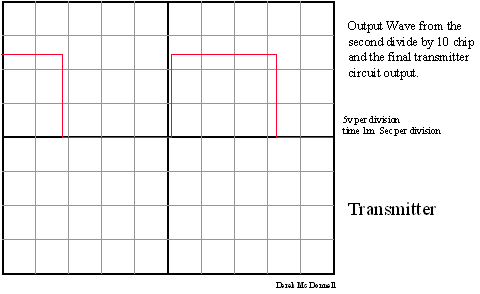
The output wave from the second divide by 10 chip is the same as the
previous wave but the frequency is divided by 10 again.
This is also the final output of the of the transmitter circuit.
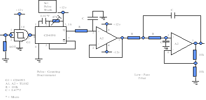
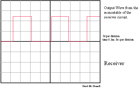
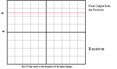
In this circuit the input gate, G1 is a Schmitt trigger NAND type;
it is included to restore the pulse waveform's shape and reduce the effects
of noise in the signal path.

The next circuit block, a CD4098 monostable, serves as a pulse-counting FM
discriminator.
The monostable produces a constant-width pulse when triggered;
a high-frequency input therefore gives an output wave with a higher DC
(average) level than does a low-frequency input signal. This DC component -
the output signal of the telemetry system - is extracted by the 3 pole lowpass
filter built around OP-AMP's A1 and A2. The filter is set to cut off at about
3 Hz as only very slow transducer movement is anticipated.

Procedure:

1)	Now build the receiver circuit, details are shown in Figure 3.0.

2)	Once again characterise each stage as it is completed, carefully
	noting waveforms and voltage levels.

3)	Confirm proper receiver operation using the oscilloscope, triggering
	the circuit from a CMOS compatible square-wave signal generator.

4)	Produce a calibration curve for the unit: plot DC output voltages
	verses input frequency.
Expected Results
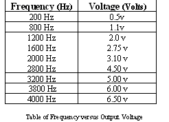
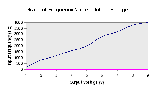
The result expected from stage one is a uniform square pulse because this chip is a 555 Timer chip. This was exactly what was received in practice. The result expected from stage two was again a square wave but with its frequency divided by 100 because of the two CD 4017 chips which dive by 10 each time. The result from stage two is got before the 470 W resistor and after the collector of the BC 108 transistor. The received wave was the same in practice as in theory. Filter Output Voltage verses Voltage to sensor Capacitance 2x1 nF Time 2mS/div, Voltage 5 volts/div > f = 71.4kHz 3x1 nF Time 5mS/div, Voltage 5 volts/div > f = 50kHz 4x1 nF Time 10mS/div, Voltage 5 volts/div > f= 38.5kHz
Conclusion

The results obtained from the circuit outputs were satisfactory and
varied only slightly with the data sheets. There were many problems
with the circuit but the most interesting one was the failure of the
transmitter to produce a strong enough signal so that the receiver
could pick up the signal at the other end.
| Send comments to webmaster Copyright © 1997 Derek Mc Donnell. All Rights Reserved. Last updated 15-Mar-1998. |
|